


Minipod style tripod for near bottom current and wave measurements ready for deployment.
Coastal and Estuarine Dynamics Project Active
By Woods Hole Coastal and Marine Science Center
December 30, 2018
Coastal and Estuarine Dynamics Project exists to support ocean, coastal and estuarine research. The staff have a broad set of skills; from instrument design and development to all forms of work at sea to software development and data management. The team has successfully deployed and recovered more than 1000 data collection platforms for research in the last 30 years.
Oceanographic Time-Series Data Collection
Oceanographic Time-Series Data Collection

Oceanographic time-series measurements made by the USGS between 1975 and the present as part of research programs. The data were collected to address specific research questions using stationary platforms with sensors near the seafloor
Research Themes
Research Themes
The Coastal and Estuarine Dynamics Group's research, projects, and equipment.
The U.S. Geological Survey (USGS) Coastal and Estuarine Dynamics Project, part of the USGS Woods Hole Coastal and Marine Science Center, provides operational support for studies of coastal ocean circulation and sediment transport. The Coastal and Estuarine Dynamics Project staff design, fabricate, deploy, and recover a variety of instrumented platforms for research. It has capabilities in engineering, software development, project management, data acquisition, data processing and data archiving. Instrument measurement quality assessments, interface design, and development of novel housings are all examples of the engineering tasks routinely completed. The Coastal and Estuarine Dynamics Project maintains a diverse pool of high-quality oceanographic instruments, and develop new techniques to improve or modify existing sensors and systems. Field experiments are conducted in estuarine, coastal, and continental shelf regions. Oceanographic moorings, tripods and other platforms are deployed at water depths ranges from less than a meter to more than a thousand meters.
The Coastal and Estuarine Dynamics Project team members have extensive experience in collecting and managing oceanographic data from deep water to near shore environments. They support research projects carried out by scientists at the USGS Woods Hole Coastal and Marine Science Center and their colleagues, with assistance to other programs as resources allow.

Sources/Usage: Public Domain. View Media Details
The data collected are typically comprised of measurements from sensors deployed in arrays at fixed locations. These time-series observations are used in studies of regional circulation and sediment transport processes in estuaries, marshes, beach regions and in the coastal ocean. The observation periods range from a few days to more than a year. Since 1975, the Coastal and Estuarine Dynamics Project has deployed over 1000 separate platforms in support of field research programs.
An extensive software system has been developed and maintained to decode, process, edit, display, archive and analyze the oceanographic data collected. This system uses Matlab® and python programs to output files in EPIC-compliant NetCDF format. CF-Compliant NetCDF files are also created and are available at [http://cfconventions.org] and the Oceanographic Time-Series Database.
Time series observations collected throughout the U.S. Exclusive Economic Zone (E.E.Z.) by the group since 1975 are managed, archived and distributed to collaborators, other investigators, and the public over the World Wide Web as part of the U.S. Geological Survey Oceanographic Time-Series Database (see http://stellwagen.er.usgs.gov). File downloads and access via OPeNDAP are possible from the page describing each experiment.

Sources/Usage: Public Domain. View Media Details
Below are other science projects associated with this project.
Coastal and Estuarine Dynamics- Equipment
The Coastal and Estuarine Dynamics Project maintains an extensive and diverse inventory of instruments for measuring oceanographic parameters in-situ over long periods of time (a few days to as long as one year) and platforms on which to deploy the instruments in estuarine, coastal, and deep ocean environments. These instruments measure a wide variety of parameters relevant to studies of sediment...
Estuarine Processes, Hazards, and Ecosystems
Estuarine processes, hazards, and ecosystems describes several interdisciplinary projects that aim to quantify and understand estuarine processes through observations and numerical modeling. Both the spatial and temporal scales of these mechanisms are important, and therefore require modern instrumentation and state-of-the-art hydrodynamic models. These projects are led from the U.S. Geological...
Coastal and Estuarine Dynamics- Projects
Field experiments carried out by the Coastal and Estuarine Dynamics Project include observations offshore of barrier islands and headlands; observations on barrier islands; observations in estuaries; observations in shelf environments; and process studies of sediment transport in the bottom boundary layer. Experiments typically involved deployment of an array of a variety of instrument systems for...
Coastal and Estuarine Dynamics - Engineering
The Coastal and Estuarine Dynamics Project primarily uses off-the-shelf instrumentation and sensors to collect observations. Coastal and Estuarine Dynamics team designs and implements novel configurations for logging of data from sensors, and for deployment of these instruments in a wide range of estuarine, coastal, and ocean environments. Project staff continually evaluates instrument and sensor...
Below are multimedia items associated with this project.
Minipod style tripod for near bottom current and wave measurements
Minipod style tripod for near bottom current and wave measurements ready for deployment.

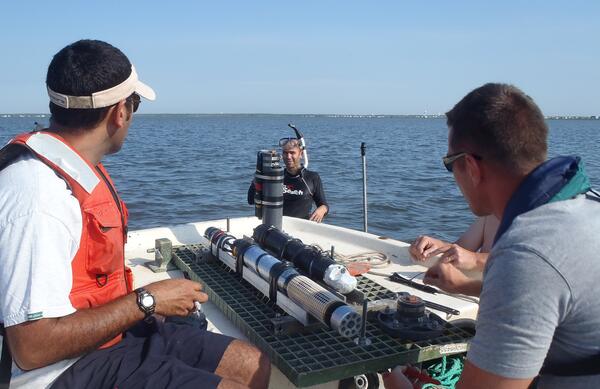
Divers prepare oceanographic equipment
Divers prepare patterns of known targets for verification of sonar resolution.
Divers prepare patterns of known targets for verification of sonar resolution.

Oceanographic Tripods on the Dock
A flow tripod (taller, right) and sonar tripod (smaller, left) at the dock before being loaded onto a ship and taken to a site off Fire Island for deployment.
A flow tripod (taller, right) and sonar tripod (smaller, left) at the dock before being loaded onto a ship and taken to a site off Fire Island for deployment.

Deployment of an instrumented quadrapod off Martha’s Vineyard
Deployment of an instrumented quadrapod off Martha’s Vineyard, November 2014.
Deployment of an instrumented quadrapod off Martha’s Vineyard, November 2014.
Marinna Martini prepares to deploy a NIMBBLE from the R/V Connecticut
Marinna Martini prepares to deploy a NIMBBLE from the R/V Connecticut south of Martha's Vineyard
Marinna Martini prepares to deploy a NIMBBLE from the R/V Connecticut south of Martha's Vineyard

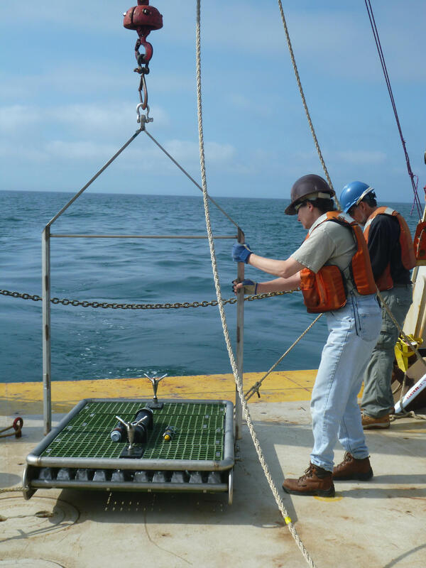
USGS technicians prepare a sediment trap
USGS technicians prepare a sediment trap to sample the sea floor off Cape Hatteras.
USGS technicians prepare a sediment trap to sample the sea floor off Cape Hatteras.
Shallow Water Irradience Platform placement in Barnegat Bay, NJ
Investigators prepare to place a Shallow Water Irradience Platform (SWIP) at a site in Barnegat Bay, NJ.
Investigators prepare to place a Shallow Water Irradience Platform (SWIP) at a site in Barnegat Bay, NJ.
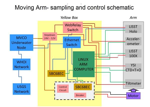
Schematic of system designed to control movement and logging of data
Schematic of system designed to control movement and logging of data collected by the Moving Arm Tripod at Martha's Vineyard Coastal Observatory in 2011.
Schematic of system designed to control movement and logging of data collected by the Moving Arm Tripod at Martha's Vineyard Coastal Observatory in 2011.

Electronics for controlling the moving arm
Electronics for controlling the moving arm in the open pressure housing.
Electronics for controlling the moving arm in the open pressure housing.

Deploying an instrumented minipod South of Fire Island, NY.
USGS researchers deploying an instrumented minipod South of Fire Island, NY.
USGS researchers deploying an instrumented minipod South of Fire Island, NY.

Remote places
Woods Hole Coastal and Marine Science Center's Ellyn Montgomery (right) on the helipad of the Canadian Coast Guard Vessel Louis St. Laurent returning from an ice reconnaissance flight as part of a joint study mapping the foot of the continental slope in the Arctic Ocean in 2008
Woods Hole Coastal and Marine Science Center's Ellyn Montgomery (right) on the helipad of the Canadian Coast Guard Vessel Louis St. Laurent returning from an ice reconnaissance flight as part of a joint study mapping the foot of the continental slope in the Arctic Ocean in 2008
Coastal and Estuarine Dynamics Project exists to support ocean, coastal and estuarine research. The staff have a broad set of skills; from instrument design and development to all forms of work at sea to software development and data management. The team has successfully deployed and recovered more than 1000 data collection platforms for research in the last 30 years.
Oceanographic Time-Series Data Collection
Oceanographic Time-Series Data Collection
Oceanographic time-series measurements made by the USGS between 1975 and the present as part of research programs. The data were collected to address specific research questions using stationary platforms with sensors near the seafloor
Research Themes
Research Themes
The Coastal and Estuarine Dynamics Group's research, projects, and equipment.
The U.S. Geological Survey (USGS) Coastal and Estuarine Dynamics Project, part of the USGS Woods Hole Coastal and Marine Science Center, provides operational support for studies of coastal ocean circulation and sediment transport. The Coastal and Estuarine Dynamics Project staff design, fabricate, deploy, and recover a variety of instrumented platforms for research. It has capabilities in engineering, software development, project management, data acquisition, data processing and data archiving. Instrument measurement quality assessments, interface design, and development of novel housings are all examples of the engineering tasks routinely completed. The Coastal and Estuarine Dynamics Project maintains a diverse pool of high-quality oceanographic instruments, and develop new techniques to improve or modify existing sensors and systems. Field experiments are conducted in estuarine, coastal, and continental shelf regions. Oceanographic moorings, tripods and other platforms are deployed at water depths ranges from less than a meter to more than a thousand meters.
The Coastal and Estuarine Dynamics Project team members have extensive experience in collecting and managing oceanographic data from deep water to near shore environments. They support research projects carried out by scientists at the USGS Woods Hole Coastal and Marine Science Center and their colleagues, with assistance to other programs as resources allow.
Sources/Usage: Public Domain. View Media Details
The data collected are typically comprised of measurements from sensors deployed in arrays at fixed locations. These time-series observations are used in studies of regional circulation and sediment transport processes in estuaries, marshes, beach regions and in the coastal ocean. The observation periods range from a few days to more than a year. Since 1975, the Coastal and Estuarine Dynamics Project has deployed over 1000 separate platforms in support of field research programs.
An extensive software system has been developed and maintained to decode, process, edit, display, archive and analyze the oceanographic data collected. This system uses Matlab® and python programs to output files in EPIC-compliant NetCDF format. CF-Compliant NetCDF files are also created and are available at [http://cfconventions.org] and the Oceanographic Time-Series Database.
Time series observations collected throughout the U.S. Exclusive Economic Zone (E.E.Z.) by the group since 1975 are managed, archived and distributed to collaborators, other investigators, and the public over the World Wide Web as part of the U.S. Geological Survey Oceanographic Time-Series Database (see http://stellwagen.er.usgs.gov). File downloads and access via OPeNDAP are possible from the page describing each experiment.
Sources/Usage: Public Domain. View Media Details
Below are other science projects associated with this project.
Coastal and Estuarine Dynamics- Equipment
The Coastal and Estuarine Dynamics Project maintains an extensive and diverse inventory of instruments for measuring oceanographic parameters in-situ over long periods of time (a few days to as long as one year) and platforms on which to deploy the instruments in estuarine, coastal, and deep ocean environments. These instruments measure a wide variety of parameters relevant to studies of sediment...
Estuarine Processes, Hazards, and Ecosystems
Estuarine processes, hazards, and ecosystems describes several interdisciplinary projects that aim to quantify and understand estuarine processes through observations and numerical modeling. Both the spatial and temporal scales of these mechanisms are important, and therefore require modern instrumentation and state-of-the-art hydrodynamic models. These projects are led from the U.S. Geological...
Coastal and Estuarine Dynamics- Projects
Field experiments carried out by the Coastal and Estuarine Dynamics Project include observations offshore of barrier islands and headlands; observations on barrier islands; observations in estuaries; observations in shelf environments; and process studies of sediment transport in the bottom boundary layer. Experiments typically involved deployment of an array of a variety of instrument systems for...
Coastal and Estuarine Dynamics - Engineering
The Coastal and Estuarine Dynamics Project primarily uses off-the-shelf instrumentation and sensors to collect observations. Coastal and Estuarine Dynamics team designs and implements novel configurations for logging of data from sensors, and for deployment of these instruments in a wide range of estuarine, coastal, and ocean environments. Project staff continually evaluates instrument and sensor...
Below are multimedia items associated with this project.
Minipod style tripod for near bottom current and wave measurements
Minipod style tripod for near bottom current and wave measurements ready for deployment.
Minipod style tripod for near bottom current and wave measurements ready for deployment.
Divers prepare oceanographic equipment
Divers prepare patterns of known targets for verification of sonar resolution.
Divers prepare patterns of known targets for verification of sonar resolution.
Oceanographic Tripods on the Dock
A flow tripod (taller, right) and sonar tripod (smaller, left) at the dock before being loaded onto a ship and taken to a site off Fire Island for deployment.
A flow tripod (taller, right) and sonar tripod (smaller, left) at the dock before being loaded onto a ship and taken to a site off Fire Island for deployment.
Deployment of an instrumented quadrapod off Martha’s Vineyard
Deployment of an instrumented quadrapod off Martha’s Vineyard, November 2014.
Deployment of an instrumented quadrapod off Martha’s Vineyard, November 2014.
Marinna Martini prepares to deploy a NIMBBLE from the R/V Connecticut
Marinna Martini prepares to deploy a NIMBBLE from the R/V Connecticut south of Martha's Vineyard
Marinna Martini prepares to deploy a NIMBBLE from the R/V Connecticut south of Martha's Vineyard
USGS technicians prepare a sediment trap
USGS technicians prepare a sediment trap to sample the sea floor off Cape Hatteras.
USGS technicians prepare a sediment trap to sample the sea floor off Cape Hatteras.
Shallow Water Irradience Platform placement in Barnegat Bay, NJ
Investigators prepare to place a Shallow Water Irradience Platform (SWIP) at a site in Barnegat Bay, NJ.
Investigators prepare to place a Shallow Water Irradience Platform (SWIP) at a site in Barnegat Bay, NJ.
Schematic of system designed to control movement and logging of data
Schematic of system designed to control movement and logging of data collected by the Moving Arm Tripod at Martha's Vineyard Coastal Observatory in 2011.
Schematic of system designed to control movement and logging of data collected by the Moving Arm Tripod at Martha's Vineyard Coastal Observatory in 2011.
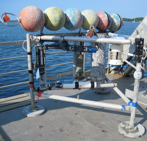
Electronics for controlling the moving arm
Electronics for controlling the moving arm in the open pressure housing.
Electronics for controlling the moving arm in the open pressure housing.
Deploying an instrumented minipod South of Fire Island, NY.
USGS researchers deploying an instrumented minipod South of Fire Island, NY.
USGS researchers deploying an instrumented minipod South of Fire Island, NY.
Remote places
Woods Hole Coastal and Marine Science Center's Ellyn Montgomery (right) on the helipad of the Canadian Coast Guard Vessel Louis St. Laurent returning from an ice reconnaissance flight as part of a joint study mapping the foot of the continental slope in the Arctic Ocean in 2008
Woods Hole Coastal and Marine Science Center's Ellyn Montgomery (right) on the helipad of the Canadian Coast Guard Vessel Louis St. Laurent returning from an ice reconnaissance flight as part of a joint study mapping the foot of the continental slope in the Arctic Ocean in 2008